High-Performance 4-Layer PCB Solutions with F4BTMS1000 Material for Demanding Applications
(Custom PCBs are tailored products; the images and specifications provided are for reference only.)
Introduction to F4BTMS1000:
The F4BTMS series represents an advanced iteration of the F4BTM series, featuring significant breakthroughs in material formulation and manufacturing processes. This high-reliability material is enriched with a substantial amount of ceramics and reinforced with ultra-thin, ultra-fine glass fiber cloth, resulting in enhanced performance and a broader range of dielectric constants. It is particularly suitable for aerospace applications and can effectively replace comparable foreign products.
By incorporating a carefully balanced mix of ultra-thin glass fiber cloth and specially distributed nano-ceramics combined with polytetrafluoroethylene resin, the negative impacts of glass fiber on electromagnetic wave propagation are minimized. This innovation reduces dielectric loss, enhances dimensional stability, and decreases anisotropy in the X/Y/Z axes. Additionally, it improves electrical strength, thermal conductivity, and exhibits excellent low thermal expansion characteristics.
Properties of F4BTMS1000:
Dielectric Constant (Dk): 10.2 at 10 GHz
Dissipation Factor: 0.0020 at 10 GHz, 0.0023 at 20 GHz
Coefficient of Thermal Expansion (CTE):
X-axis: 16 ppm/°C
Y-axis: 18 ppm/°C
Z-axis: 32 ppm/°C (from -55°C to 288°C)
Low Thermal Coefficient of Dk: -320 ppm/°C (from -55°C to 150°C)
High Thermal Conductivity: 0.81 W/mK
Low Moisture Absorption: 0.03%
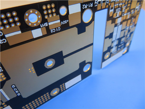
PCB Construction Details:
| Specification | Details |
|---|---|
| Base Material | F4BTMS1000 |
| Layer Count | 4 layers |
| Board Dimensions | 145mm x 145mm (± 0.15mm) |
| Minimum Trace/Space | 5/7 mils |
| Minimum Hole Size | 1.2mm |
| Blind Vias | Top to Inner Layer 1; Buried: Inner Layer 2 to Inner Layer 3 |
| Finished Board Thickness | 12.9mm |
| Finished Copper Weight | 1 oz (1.4 mils) for inner and outer layers |
| Via Plating Thickness | 20 µm |
| Surface Finish | HASL (Hot Air Solder Leveling) |
| Top Silkscreen | White |
| Bottom Silkscreen | No |
| Top Solder Mask | Black |
| Bottom Solder Mask | No |
| Electrical Testing | 100% Electrical Testing conducted prior to shipment |
PCB Stackup:
Copper Layer 1: 35 µm
F4BTMS1000 Core: 6.35 mm (250 mil)
Copper Layer 2: 35 µm
Prepreg RO4450F: 0.102 mm (4 mil)
Copper Layer 3: 35 µm
F4BTMS1000 Core: 6.35 mm (250 mil)
Copper Layer 4: 35 µm
PCB Statistics:
Components: 19
Total Pads: 77
Through Hole Pads: 35
Top SMT Pads: 42
Bottom SMT Pads: 0
Vias: 32
Nets: 2
Artwork and Standards Information
Type of Artwork Supplied: Gerber RS-274-X
Accepted Standard: IPC-Class-2
Availability: Worldwide
Typical Applications:
Aerospace equipment and cabin systems
Microwave and RF applications
Military radar systems
Feed networks
Phase-sensitive and phased array antennas
Satellite communications and more
